What is ASIC design in VLSI?
What is ASIC design in VLSI?
ASIC design flow is a mature and silicon-proven IC design process which includes various steps like design conceptualization, chip optimization, logical/physical implementation, and design validation and verification.
What is the design flow of VLSI design?
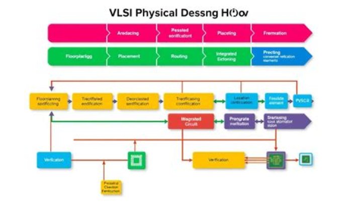
The VLSI design cycle starts with a formal specification of a VLSI chip, follows a series of steps, and eventually produces a packaged chip. A typical design cycle may be represented by the flow chart shown in Figure. Our emphasis is on the physical design step of the VLSI design cycle.
What is ASIC physical design?
ASIC Physical design is sometimes called “back-end design” because it follows the “front-end” which is generally the first part of any ASIC design. ASIC Physical Design is the part where the design meets the physical world and therefore also the real world constrains, performance and behaviour.
What is full custom ASIC design flow?
Full-custom design is a methodology for designing integrated circuits by specifying the layout of each individual transistor and the interconnections between them. The main factor affecting the design and production of ASICs is the high cost of mask sets and the requisite EDA design tools.
What is the physical design flow of VLSI system?
VLSI Physical Design Flow is an algorithm with several objectives. Some of them include minimum area, wire length and power optimization. It also involves preparing timing constraints and making sure, that netlist generated after physical design flow meets those constraints.
What is flow in VLSI?
The VLSI design flow can be divided into two parts: Frontend design flow and Backend design flow. Both together, allow the creation of a functional chip from scratch to production. The frontend flow will be briefly described, while the backend flow is further analyzed.
How many types of domains are there in VLSI design flow?
A single hierarchy may not be sufficient to describe the VLSI design process. There are three design domains namely behavioral domain, structural domain and physical domain each with its own hierarchy.
What is physical design flow in VLSI?
How is physical design in VLSI?
In VLSI, physical design (is also known as integrated circuit layout) is a process in which the front end design transfer the structural netlist to the back end design team to convert into a physical layout database which consists of geometrical design information for all the physical layers which is used for …
What is the difference between ASIC and FPGA?
Even if you’re new to the field of very large-scale integration (VLSI), the primary difference between ASICs and FPGAs is fairly straightforward. An ASIC is designed for a specific application while an FPGA is a multipurpose microchip you can reprogram for multiple applications.
What is FPGA in VLSI?
The full form of FPGA is “Field Programmable Gate Array”. It contains ten thousand to more than a million logic gates with programmable interconnection. Programmable interconnections are available for users or designers to perform given functions easily.